Our team makes use of equipments based on high-power femtosecond laser to study light-matter interactions at nanometer scale through ultra-high time-resolved and spatial-resolved approaches. At present, we are mainly focusing on directions related to low-dimensional excitonic physics, including excitonic upconversion, excitonic spatial diffusion, excitonic relaxation dynamics and coupling between excitons and plasmons. The material systems involved include two-dimensional materials, metal nanostructures, dielectric structures, etc.
Transient absorption spectroscopy
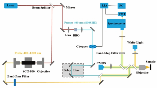
Time-resolved spectroscopy plays an essential role in physics, chemistry, biology and other fields. It is an effective approach to study the dynamics of physical processes such as charge transfer, energy transfer, carrier relaxation, etc. The common time-resolved methods to characterize optical processes are Time-Resolved Photoluminescence Spectroscopy (TRPL) and Transient absorption spectroscopy (TAS). TRPL based on pulsed laser to excite the sample, streak camera, single photon counter and other time-resolved devices are used to collect PL signals generated by sample excited, and records time intervals between the arrival of laser pulse and the PL signal is collected, so as to achieve the time-resolute purpose. However, TRPL has two obvious disadvantages. On the one hand, since TRPL collects radiative PL signals, it can only realize the time-resolved analysis of radiative process, information of non-radiative process cannot be given. On the other hand, due to the time-response limitation of electrical instruments, the time resolution limits of TRPL are generally higher than picosecond, which is suitable for the characterization of nanosecond processes. However, physical processes occur in subpicosecond scale cannot be seen, such as hot electron relaxation, charge transfer, Auger recombination, biexciton annihilation, etc. TAS uses two femtosecond pulses with relative delay, pump light and probe light, to adjust the optical path difference between pump and probe light through devices such as a displacement station, and collect the absorptivity of samples to probe light with the change of pump-probe time interval (Figure below). The information of non-radiation process can be given, and time resolution of femtosecond can be achieved at the same time.

Optical path of transient absorption pump-probe detection system
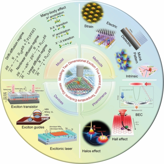
Two-dimensional excitonic physics and excitonic devices
Electrons and photons, carriers of energy and information, are of central importance in the current generation of optoelectronic elements and devices. Owing to the unique talents of electrons and photons, the efficient photonic communication and electronic processing of signals have been proved as the essential and core components the information technology. Electrons as charged particles are sensitive to surroundings because of strong Coulomb interaction, leading to the bottleneck of nanosecond response time for integrated electric devices. The electronic response time and the conversation between photonic and electronic systems inevitably limit the operation speed in the conventional optoelectronic. Thus developing compact photonic devices performing the essential logic operations is promising to accelerate information transmission and processing. The high integration of photonic devices is challenging due to the optical diffraction limit. Although there are devices have achieved switching speeds exceeding several gigahertz, high packing density is greatly limited by their active-region dimensions of 10–100 µm.
Excitons, or bound electron−hole pairs, are hydrogen-like bosonic quasiparticles with a Bohr radius of nanometer dimension, potentially combining advantages of electrons and photons. Due to its potential advantages of high operation and interconnection speed, small dimensions, and the opportunity to integrate, the optoelectronic devices operating with excitons have attracted enormous interest. Therefore, various prototypical excitonic functional devices, including modulators, storage devices, field-gradient devices, and transistors, have been envisaged and demonstrated in bulk semiconductor-based coupled quantum wells in past decades. However, the low temperature required for operation limits their practical application.
In the past decade, atomically thin transition metal dichalcogenide (TMD) semiconductors have received significant interest among numerous 2D materials owing to fascinating physical properties. Due to the reduced dielectric screening, enhanced Coulomb interactions, and relatively large effective masses of charge carriers, the electron-hole pairs formed in TMDC monolayer have ≈1 nm Bohr radius and ≈500 meV binding energy—over an order of magnitude larger than conventional semiconductors, enabling the manipulation of exciton at room temperature. Additionally, the time-reversal symmetry, broken inversion symmetry, and strong spin-orbit splitting in TMDC monolayer provide an alternative steerable degree of freedom—valley pseudospin, which can be utilized for information storage and processing, and thereby renovate modern charge- and spin-based technologies. Therefore, the atomically thin TMDC semiconductors provide an excellent platform for pursuing room temperature excitonic devices.

Adv. Mater. Technol. 7, 2200032 (2022)
Representative works:
[1] Adv. Funct. Mater. 26: 6394-6401 (2016).
[2] Light Sci Appl 8, 9 (2019).
[3] ACS Nano 14, 6, 6897–6905 (2020).
[4] eLight 1, 6 (2021).
[5] Light Sci Appl 11, 176 (2022).